Detailed hardware information for each cluster can be found on their respective page:
-
Tuolumne in the CZ
-
RZAdams in the RZ
-
El Capitan in the SCF
A comparison of ATS-4 machines
| El Capitan | Tuolumne | El Dorado* | RZAdams | |
|---|---|---|---|---|
| Nodes | 11,136 | 1,152 | 384 | 128 |
| MI300As per node | 4 | 4 | 4 | 4 |
| MI300As total | 44,544 | 4,608 | 1,536 | 512 |
| Node Peak (DP TFLOP/s) | 250.8 | 250.8 | 250.8 | 250.8 |
| System Peak (DP PFLOP/s) | 2,792.9 | 288.4 | 96.3 | 32.1 |
| System Peak (SP PFLOP/s) | 3,688.2 | 381.5 | 127.2 | 42.4 |
| System Peak (HP PFLOP/s) | 17,639.4 | 1,824.8 | 608.2 | 202.8 |
| Node Memory (GiB) (All HBM3) | 512 | 512 | 512 | 512 |
| System Memory (TiB) | 5,568 | 576 | 192 | 64 |
| Compute cabinets | 87 | 9 | 3 | 1 |
| Peak Power (MW) | 34.8 | 3.6 | 1.2 | 0.4 |
| Total Rabbit Modules | 696 | 72 | 24 | 8 |
| November 2024 Top500 position | 1 | 10 | 20 | 49 |
*El Dorado is sited at Sandia National Labs
Systems Overview
Each of the El Capitan system uses the same building blocks for computing: APUs (CPU+GPU), nodes, system interconnect, file system. Compute nodes contains 4 AMD MI300A, each allocated to its own socket with 128 GB of RAM per socket (defining a NUMA domain) for a total of 512 GB/node.
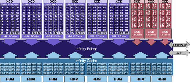
The MI300A APU consists of a combination of CPU and GPU chiplets and shared AMD Infinity Cache memory-side cache, eight stacks of HBM3, I/O interfaces, and the Infinity Fabric (IF) interconnect to provide the data movement among these components. The architecture repartitions the compute, memory, and communication elements of the processor across a heterogeneous package. The MI300A integrates 6 vertically stacked accelerator complex dies (XCD) and 4 I/O dies (IOD) containing system infrastructure, tied together with the AMD Infinity Fabric, and connecting to 8 stacks of high-bandwidth memory (HBM3).
The figure below shows a block diagram view of the MI300A APU. The MI300A has a total of six accelerator complex dies (XCDs) that operate as parallel GPU engines. The MI300A APU has three CPU complex dies (CCDs) that provide the CPU cores. The XCDs and CCDs all connect to the Infinity Fabric interconnect. The CCDs and XCDs share a unified HBM3-based memory System that enables direct load-store accesses to the HBM by either type of processor without any data copying. The CPUs are hardware coherent with all CPUs and GPUs . GPU cache coherency uses two mechanisms - directory-based cache coherency hardware within a socket and software based coherency across sockets.
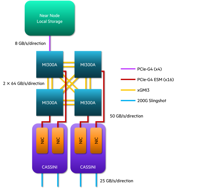
Each processor is fully connected to its peers using two AMD Infinity Fabric links with 256GB/s of bandwidth.
CDNA 3 Memory Architecture
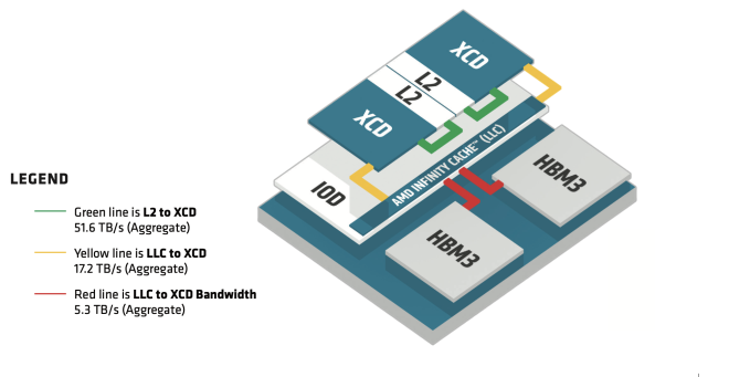
This figure displays the CDNA3 memory architecture
The L2 is a 4MB and 16-way set associative cache that is massively parallel with 16 channels that are each 256KB. The L2 cache is shared by all 38 Compute Units and services requests from both the lower level instruction and data caches. On the read side each channel can read out a 128-byte cache line and the L2 cache can sustain four requests from different CUs per cycle for a combined throughput of 2KBytes/clock for each XCD. The 16 channels support a half-line 64-byte write each with one fill request from the Infinity Fabric per clock cycle. CDNA 3 has collectively up to eight instances and up to 34.4 TB/s aggregate read bandwidth. The L2 is a writeback and write-allocate design that is intended to coalesce and reduce the number of accesses that spill out and cross the AMD Infinity Fabric to the AMD Infinity Cache. The L2 itself is coherent within an XCD. The Infinity Cache includes a snoop filter covering the multiple XCD L2 caches so that the vast majority of coherent requests from other XCDs will be resolved at the Infinity Cache without disturbing the highly utilized L2 caches.
The AMD Infinity Cache is a new infrastructure for the AMD CDNA 3 architecture that increases cache bandwidth while reducing the number of off-chip memory accesses. The AMD Infinity Cache is a shared memory-side cache, meaning that it caches the contents of memory and cannot hold dirty data evicted from a lower level cache. This has two significant benefits. First, the AMD Infinity Cache doesn’t participate in coherency and does not have to absorb or handle any snoop traffic, which significantly improves efficiency and reduces the latency of snooping from lower level caches. Second, it can hold nominally uncacheable memory such as buffers for I/O.
The AMD Infinity Cache is based on the channel concept and is 16-way set-associative. Each stack of HBM memory is associated with 16 parallel channels. A channel is 64-bytes wide and connects to 2 MB of data arrays that are banked to sustain simultaneous reads and writes. In total, there are eight stacks of HBM across the four IODs, for 128 channels or 256MB of data. The peak bandwidth from the Infinity Cache is 17.2 TB/s .
Each IOD fans out through the package to two stacks of memory. The AMD CDNA 3 uses the latest HBM3 interface. The memory controllers drive a bus that operates at 5.2 Gbps and each stack contains 16GB or 24GB of memory. Collectively, the HBM3 memory is 128GB on MI300A per socket with 5.3 TB/s peak theoretical memory bandwidth
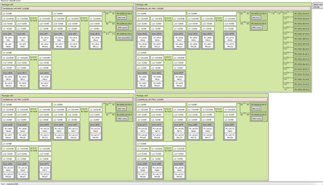
The figure below shows how the linux utility lstopo visualizes an El Cap compute node.
CPUs
Each APU has 24 Zen4 x86 CPU cores supporting the X-86 instruction set and AVX-512 and BFloat16 extensions. Each CCD has 8 Zen cores that share a 32 MB L3 cache. More information on the Zen4 CPU cores can be found on the AMD web pages.
GPUs
Each El Capitan system compute node contains 4 AMD MI300A APUs. Each APU has 6 XCD that serve as the GPUs. The AMD MI300A has a theoretical peak performance of 61.3 TFLOPS in vector double-precision.
The figure below is a logical/architectural block diagram of the MI300A APU showing the 6 XCDs, each with 38 Compute Units (CUs).
MI300A Peak Performance
|
FP64 Vector (TFLOPS) |
61.3 |
|
FP32 Vector (TFLOPS) |
122.6 |
|
FP64 Matrix (TFLOPS) |
122.6 |
|
FP32 Matrix (TFLOPS) |
122.6 |
Accelerator Complex Die (XCD)
The figure below shows a conceptual block diagram of the accelerator complex die (XCD)
Each XCD contains a shared set of global resources such as the scheduler, hardware queues, and four Asynchronous Compute Engines (ACE) that send compute shader workgroups to the Compute Units (CUs) that are the computational heart of the AMD CDNATM 3 architecture. The four ACEs are each associated with 40 CUs, although at the aggregate level there are only 38 CUs active, with 2 disabled for yield management. The 38 CUs all share a 4MB L2 cache that serves to coalesce all the memory traffic for the die.
System Interconnect
HPE Slingshot Interconnect switches – uses Dragonfly topology.
- High radix, 64-port, 25.6 Tb/s bidirectional bandwidth switch
- Each Port can deliver a unidirectional bandwidth of up to 200 Gbps (25 GB/s)
- Four HPE Slingshot 200 GbE Interfaces per node
- Total nodal injection bandwidth of 100 GB/s


